12th Grade > Physics
SEMICONDUCTORS MCQs
Total Questions : 30
| Page 3 of 3 pages
Answer: Option A. -> OR gate
:
A
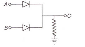
The circuit represents OR gate, as the output at C is 1, when either A or B or both A and B have input at level 1. But output at C is zero, when both A and B are at zero level and the Boolean expression is C = (A + B).
:
A
The circuit represents OR gate, as the output at C is 1, when either A or B or both A and B have input at level 1. But output at C is zero, when both A and B are at zero level and the Boolean expression is C = (A + B).
Answer: Option B. -> b
:
B
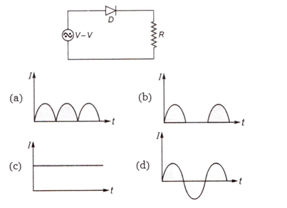
The given circuit works is half wave rectifier. In this circuit, we will get current through R when p-n junction diode is forward biased and no current when p-n junction is reversed biased. Thus the current through resistance will be shown by graph (b).
:
B
The given circuit works is half wave rectifier. In this circuit, we will get current through R when p-n junction diode is forward biased and no current when p-n junction is reversed biased. Thus the current through resistance will be shown by graph (b).
Answer: Option A. -> βAC=△IC△IB,VC=constant
:
A
It is βAC=△IC△IB,VC=constant
Collector voltage is to be kept a constant.
:
A
It is βAC=△IC△IB,VC=constant
Collector voltage is to be kept a constant.
Answer: Option B. -> 49
:
B
Ib=Ie−Ic = 5.60 - 5.488 = 0.112mA
β=IeIb=5.4880.112 = 49.
:
B
Ib=Ie−Ic = 5.60 - 5.488 = 0.112mA
β=IeIb=5.4880.112 = 49.
Answer: Option D. -> 80 mA
:
D
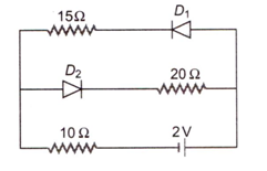
In the given circuit, junction diode D1 if forward biased, will conduct current and junction diode D2 is reverse biased, will not conduct current. Therefore, current
I = 210+15 = 0.08 A = 80 mA.
:
D
In the given circuit, junction diode D1 if forward biased, will conduct current and junction diode D2 is reverse biased, will not conduct current. Therefore, current
I = 210+15 = 0.08 A = 80 mA.
Answer: Option A. -> 1, 0, 1
:
A
The output of OR gate is
Y’ = (A + B)
The output and AND gate is
Y = Y’ . C = (A + B) . C
IfA = 1, B = 0, C = 1, they Y = (1 + 0). 1 = 1
:
A
The output of OR gate is
Y’ = (A + B)
The output and AND gate is
Y = Y’ . C = (A + B) . C
IfA = 1, B = 0, C = 1, they Y = (1 + 0). 1 = 1
Answer: Option C. -> Ic
:
C
∝=IcIe<1 or Ic<Ie
:
C
∝=IcIe<1 or Ic<Ie
Answer: Option C. -> 600
:
C
Av=βRoRi=60×5000500 = 600
:
C
Av=βRoRi=60×5000500 = 600
Answer: Option C. -> 19
:
C
β=∝1−∝=0.951−0.95=0.950.05 = 19
:
C
β=∝1−∝=0.951−0.95=0.950.05 = 19


