Sail E0 Webinar

11th And 12th > Physics

SEMICONDUCTORS MCQs

Total Questions : 30 | Page 3 of 3 pages
Question 21.


How many NAND gates are used in an OR gate?


  1.     Four
  2.     Two
  3.     Three
  4.     Five
 Discuss Question
Answer: Option C. -> Three
:
C

For this purpose we use three NAND gate in manner as shown. The first two NAND gates are operated as NOT gates and their outputs are fed to the third. The resulting circuit is OR gate.
How Many NAND Gates Are Used In An OR Gate?


Question 22.


A p-n junction (D) shown in the figure can act as a rectifier. An alternating current source (V) is connected in the circuit. The current (I) in the resistor (R) can be shown by A P-n Junction (D) Shown In The Figure Can Act As A Rectifie...


  1.     a
  2.     b
  3.     c
  4.     d
 Discuss Question
Answer: Option B. -> b
:
B

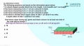
The given circuit works is half wave rectifier. In this circuit, we will get current through R when p-n junction diode is forward biased and no current when p-n junction is reversed biased. Thus the current through resistance will be shown by graph (b).


Question 23.


To get an output Y = 1 from the circuit shown in figure the inputs A, B and C must be respectively  To Get An Output Y = 1 From The Circuit Shown In Figure The ...


  1.     1, 0, 1
  2.     1, 1, 0
  3.     0, 1, 0
  4.     1, 0, 0
 Discuss Question
Answer: Option A. -> 1, 0, 1
:
A

The output of OR gate is


            Y’ = (A + B)


The output and AND gate is


            Y = Y’ . C = (A + B) . C


If  A = 1, B = 0, C = 1, they Y = (1 + 0). 1 = 1


Question 24.


In an unbiased p-n junction,


  1.     potential at p is equal to that at n   
  2.     potential at p is +ve and that at n is –ve  
  3.     potential at p is more than that at n
  4.     potential at p is less than that at n
 Discuss Question
Answer: Option D. -> potential at p is less than that at n
:
D

Option (d)
At the barrier, there are electron concentration on p side.


Question 25.


A Si and a Ge diode has identical physical dimensions. The band gap in Si is larger than that in Ge. An identical reverse bias is applied across the diodes


  1.     The reverse current in Ge is larger than that in Si          
  2.     The reverse current in Si is larger than that in Ge
  3.     The reverse current is identical in the two diodes          
  4.     The relative magnitude of the reverse currents cannot be determined from the given data only
 Discuss Question
Answer: Option C. -> The reverse current is identical in the two diodes          
:
C

When a diode is reverse biased, then the applied voltage supports the barrier voltage. Due to it, the reverse current is weak. It will be identical in two diodes.


Question 26.


The combination of the following gates produces
 The Combination Of The Following Gates Produces 


  1.     AND gate
  2.     NAND gate
  3.     NOR gate
  4.     OR gate
 Discuss Question
Answer: Option A. -> AND gate
:
A

Output of first NAND gate is, Y=¯¯¯¯¯¯¯¯¯¯¯A.B
Output of second NAND gate is,
Y=¯¯¯¯Y=¯¯¯¯¯¯¯¯¯¯¯¯¯¯¯¯¯¯¯¯¯¯A.B=A.B
Thus AND gate is formed.


Question 27.


In common base mode of transistor, the collector  current is 5.488 mA for an emitter current of 5.60 mA. The value of the base current amplification factor (β) will be


  1.     48
  2.     49
  3.     50 
  4.     51
  5.     35 mA
 Discuss Question
Answer: Option B. -> 49
:
B

Ib=IeIc = 5.60 - 5.488 = 0.112 mA
β=IeIb=5.4880.112 = 49.


Question 28.


In the circuit as shown in figure, A and B represent two inputs and C represents the
 In The Circuit As Shown In Figure, A And B Represent Two Inp...


  1.     OR gate
  2.     NOR gate
  3.     AND gate
  4.     NAND gate
  5.     35 mA
 Discuss Question
Answer: Option A. -> OR gate
:
A

The circuit represents OR gate, as the output at C is 1, when either A or B or both A and B have input at level 1. But output at C is zero, when both A and B are at zero level and the Boolean expression is C = (A + B).


Question 29.


The current I through 10 Ω resistor in the circuit shown in figure.
 The Current I Through 10 Ω Resistor In The Circuit Shown In...


  1.     50 mA
  2.     20 mA
  3.     40 mA
  4.     80 mA
  5.     35 mA
 Discuss Question
Answer: Option D. -> 80 mA
:
D

In the given circuit, junction diode D1 if forward biased, will conduct current and junction diode D2 is reverse biased, will not conduct current. Therefore, current
I = 210+15 = 0.08 A = 80 mA.


Question 30.


A working transistor with its three legs marked P, Q and R is tested using a multi-meter. No conduction is found between P and Q. By connecting the common (negative) terminal of the multimeter to R and the other (positive) terminal to P or Q, some resistance is seen on the multi-meter.  Which of the following is true for the transistor?


  1.     It is an n-p-n transistor with R as collector
  2.     It is an n-p-n transistor with R as base     
  3.     It is an p-n-p transistor with R as collector  
  4.     It is an p-n-p transistor with R as emitter
  5.     35 mA
 Discuss Question
Answer: Option B. -> It is an n-p-n transistor with R as base     
:
B

When a multimeter is connected between P and Q there is no conduction between P and Q, then P and Q are of same type of semiconductor, ie, either both are on n-type or of p-type. It means emitter and collector of a transistor are P and Q. When R is connected to negative terminal of multimeter and positive terminal to P or Q, then emitter-base junction will conduct to some extent due to reverse biasing.


The similar is the case of collector – base junction. Thus the transistor is n-p-n transistor with R as base.


Latest Videos

Latest Test Papers